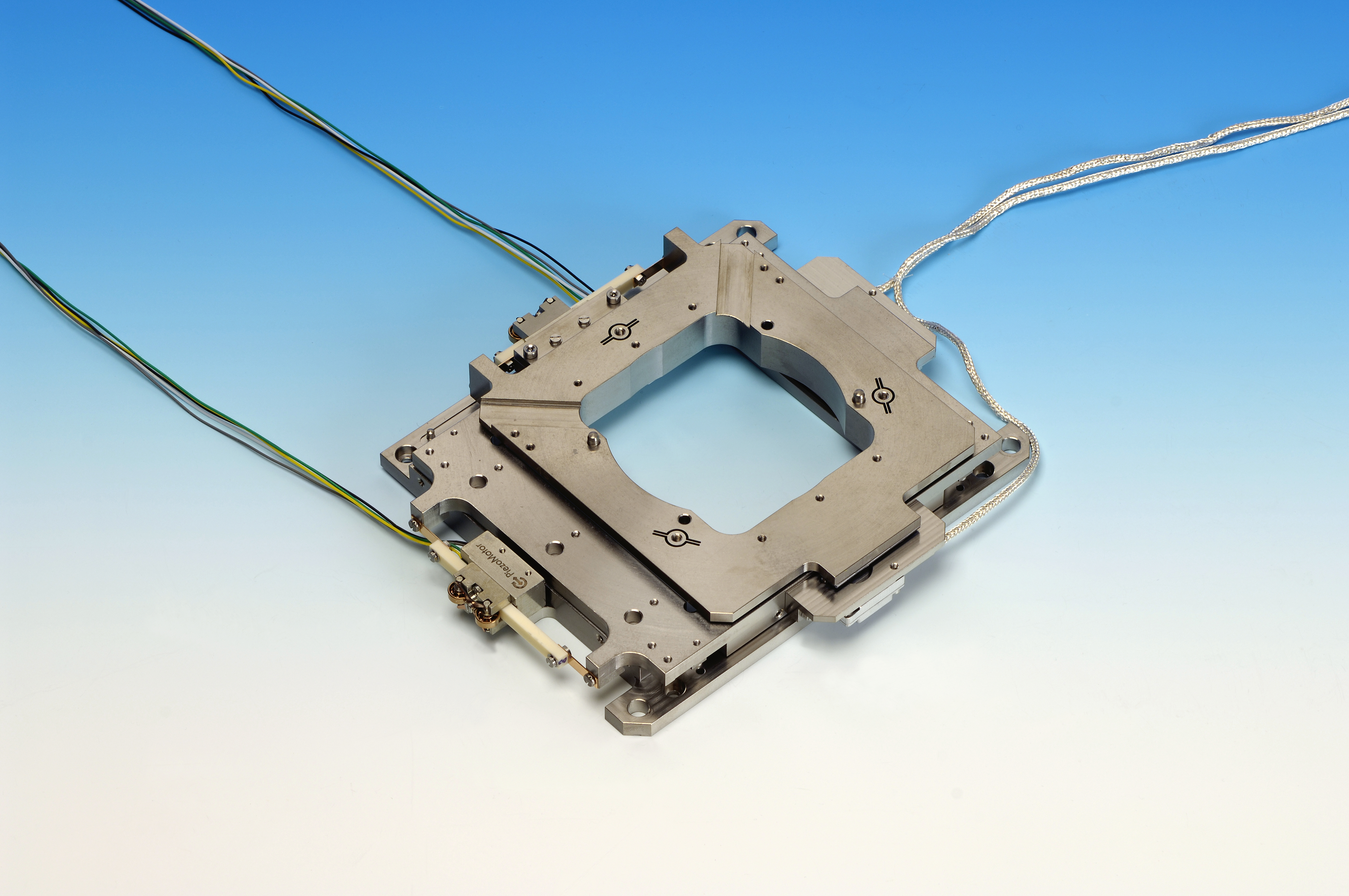
Fraunhofer IOF has many years of expertise in the field of developing and building sophisticated optical micro- and nano-structures. The key technology it uses is electron-beam lithography. Thanks to its small spot sizes – a few nanometers – electron-beam lithography is an ideal tool for nanotechnology. The technological equipment the institute has enables it to efficiently generate optical micro- and nano-structures on surfaces up to 300 mm in size with the highest precision and resolution.
Contact Press / Media
Dr. Uwe Zeitner
Fraunhofer Institute for Applied Optics and Precision Engineering IOF
Albert-Einstein-Str. 7
07745 Jena
Phone +49 3641 807-403
Fax +49 3641 807-603

