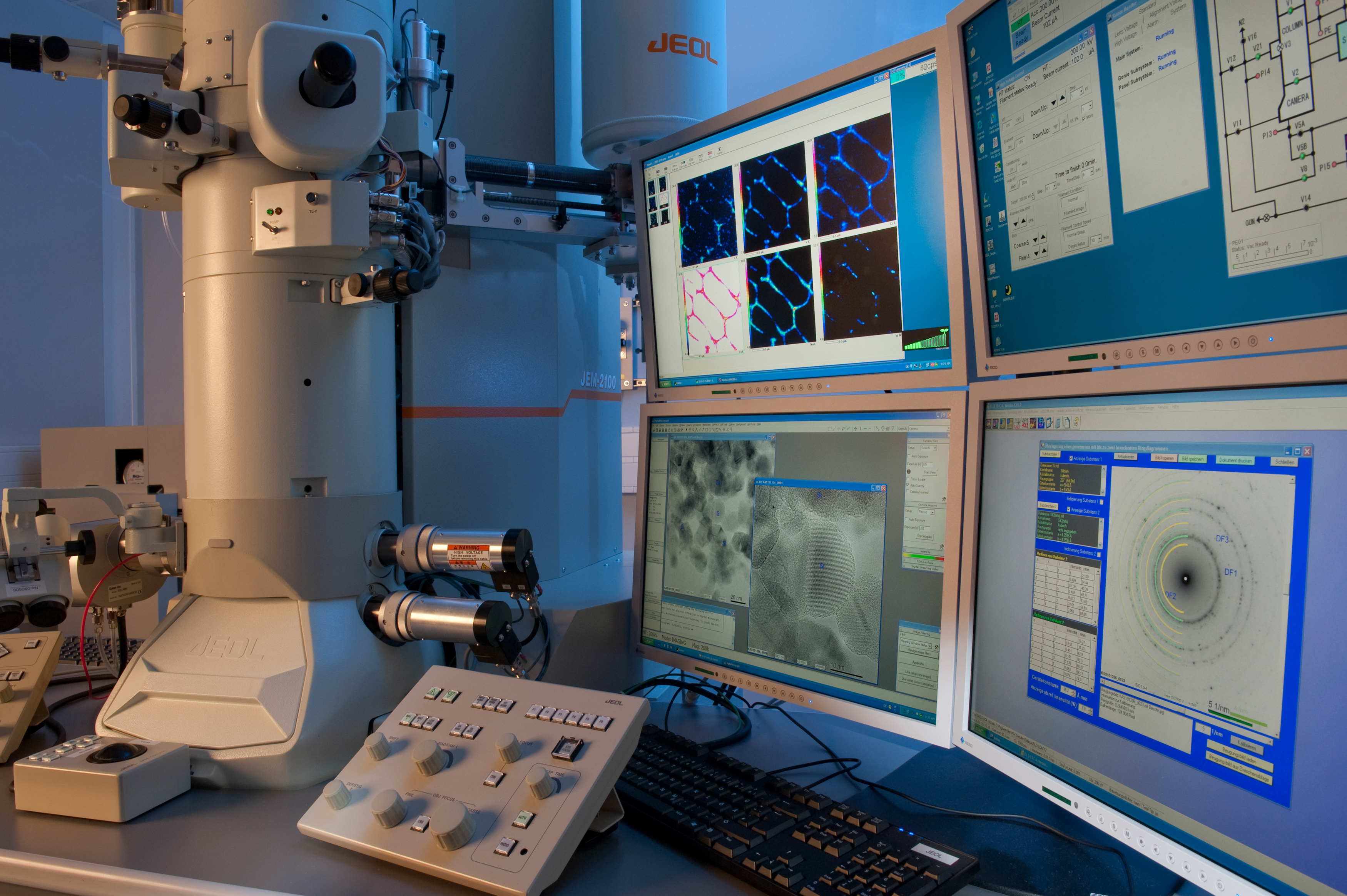
To successfully develop a processing method, research needs to conduct a detailed analysis of the processing results as well as a comprehensive characterization of the initial requirements and material contexts. All institutes of the Fraunhofer Group for Light & Surfaces have suitable measuring methods and material examination methods to accomplish this.
Thin Film Characterization
To characterize thin films, Fraunhofer IST has a wide range of material characterization processes, e.g. for chemical analysis of materials (spatially resolved, deep-resolved, near-surface or averaged). These include X-ray spectroscopy (EDX/WDX/EPMA), secondary ion mass spectroscopy (SIMS), photoelectron spectroscopy (XPS), and X-ray fluorescence analysis (RFA/XRF). Crystalline materials can also be examined by X-ray diffraction (XRD). In addition, various microscopes are available for surface imaging: confocal laser microscopy (CLM), scanning force microscopy (AFM) and scanning electron microscopy (SEM) with focused ion beam (FIB).
Material Analysis
Furthermore, there are numerous application-specific test methods for characterizing material properties, e.g. hardness, friction, wear, corrosion, or fatigue behavior. Spectroscopy, ellipsometry, color and scattered light measurements are also available for characterizing many optical properties.
For technology development and quality assessment, Fraunhofer IWS and Fraunhofer ILT provide state-of-the-art equipment for mechanical-technological tests, metallography, light and electron microscopy as well as microanalysis. They share many years of experience in characterizing edge-treated and welded samples and components made of metallic materials, as well as in analyzing layers, layer systems, nanoparticles and nanotubes.
Besides conducing material investigations, the institutes can also carry out functional investigations on components. The range extends from determining mechanical characteristics of materials and material combinations, to calculating characteristic curves for the evaluation of vibration resistance and, in particular, conducting time-shortened fatigue tests at high test frequencies. Furthermore, the institutes can analytically characterize laser-modified edge zones, joining interfaces, thin-film systems, nanotubes and nanoparticles all in high-resolution images.
Fraunhofer FEP has a wide range of methods to characterize thin films and surfaces. The methods and extensive analytical experience of its employees are available for product and technology development. Typical application fields are layers for optics, sensors, displays, photovoltaics, packaging, corrosion and wear protection.
For the analysis of structure and microstructures, high-resolution systems are available, such as:
- Field emission scanning electron microscopy
- Ion preparation of cross sections
- Metallographic preparation technology
The analysis of topography, surface, and layer thickness is carried out using:
- Atomic force microscopy
- Profillometry
- Calotests
- Contact angles
For hermetic packaging, e.g. for OLED modules, permeation barrier measurements are available for measuring the water vapor permeability and oxygen permeability.
The analysis of optical, mechanical and electrical properties takes place with regard to:
- Hardness and elasticity modulus
- Layer tensions
- Adhesion
- Abrasion resistance,
- I-U characterisitc cure measurement of solar cells
- Quantum efficiency measurement
- Light and darkening conductivity
- Four-point measuring station
In addition, the institutes can also carry out corrosion tests and climatic tests using corrosion testing systems and climatic chambers.

