Selective Laser Melting
Powder-bed processes, which include, among others, Selective Laser Melting (SLM), are preferred when components with the highest degree of geometrical freedom need to be manufactured:
- Maximum component size: 300 x 300 x 200 mm³
- Shape accuracy: 0.1 to 1 mm.
The material spectrum that can be processed free of defects ranges from steels to nickel and cobalt alloys, as well as titanium light-weight materials all the way to carbide metals and ceramics. In addition to material investigations, Fraunhofer IWS and Fraunhofer ILT are also working on increasing feed rate and productivity. The aim at Fraunhofer IWS, for example, is to achieve processing speeds that are comparable to electron-beam welding in order to increase the efficiency of the process up to build rates > 20 cm³/h. In comparison, Frauhnofer ILT is pursuing multibeam approaches with several fiber and diode lasers in order to achieve high build rates.
Electron-Beam Melting
In the case of electron-beam melting (EBM), instead of the laser beam, an electron beam is guided across the powder coating, which may consist of ceramic and metallic powders. In comparison to the galvanic scanners of laser-assisted machining, the radiation in EBM can be manipulated very quickly through adapting electrical fields so that high feed rates of approx. 8000 m/s can be reached. This way, the process achieves high productivity and efficiency with build ratios between 55 and 80 cm³/h. The main applications currently lie in the standard processing of Ti6Al4V, Ti6Al4V ELI, TiCP Grade 2 and ASTM F75 for the manufacture of implants and components for aerospace applications.
Compared to SLM processes, however, this type of processing causes a substantially higher surface roughness, which is typically in the range of 20 to 40 μm. This means that post-processing is required in order to reduce the roughness for the desired technical surface quality.
Laser Metal Deposition
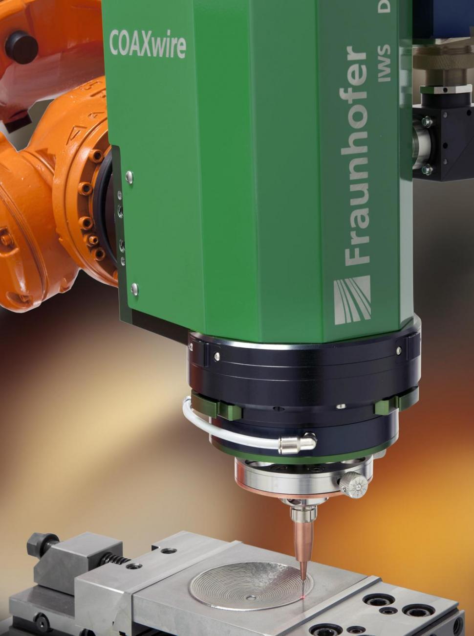
In Laser Metal Deposition (LMD), powdered additive materials are melted onto a component with a laser beam feeding the powder through a nozzle. The desired geometry is formed by as the laser traverses fixed tracks and acquires its three-dimensional contour as tracks or weld beads are superimposed. Laser Metal Deposition can be combined with local inductive heating, and the group’s developmental work here aims to generate a process that is efficient and produces components with high quality and accuracy. Furthermore, the group is advancing the scaling of the LMD process to generate microstructures < 100 μm. Both light metal and nickel superalloys, steel and intermetallic materials as well as hard material systems (carbides) are currently being processed.
Services:
- Material and process development
- Production of machining heads and integration into plants
- Process monitoring
- Creation of plant designs
- Launching production and on-site user support.
Laser Sintering
In addition to purely melting processes, sintering processes are also used in which the produced components are brought into the final shape by sintering after layered printing. Fraunhofer IOF uses additive manufacturing processes such as Selective Laser Sintering to produce specially designed light weight structures for high-quality metal optics.
Printing Technology
This work focuses developing paste-based and ink-based processes that enable 3D multi-material printing, as well as the additive production of polymer and polymer-composite structures by printing processes based on fused deposition modeling. The range of materials that can be processed for dispensing and aerosol printing is very wide since all materials that can be converted into stable pastes or inks are suitable. These include, for example, metals, semiconductors, polymers or nanoparticle-containing dispersions, as well as ceramics and composites. Plasma or laser technologies are used for the following sintering or drying steps.
In addition, new approaches are being developed for polymer-based additive processes in the field of polymerization technology. Here the group focuses on new optical approaches for stereolithography and digital light processing, with which it expects to increase the process speed considerably. Furthermore, process and system developments for multi-photon lithography are being pursued in order to produce structures in the range < 1 μm. These works are combined by material developments, e.g. new Thiol-Ene compositions, which enable high functionality without initiators and allow a wide variety of polymer compositions to be generated.
The Fraunhofer IOF and the Fraunhofer ILT institutes are examining technologies to print wiring structures made of silver and gold as well as materials suitable for actuators. However, even in life science applications such as lab-on-chip systems for patient-related diagnostics, printed actuator structures are of interest, for example for chip-integrated pumps and valves.
Services:
- Production of pure mechanical 3D structural components
- Printing of highly complex electronic structures, such as thermoelectric generators, sensors, batteries, or printed circuit boards for high-performance electronics
- Integration of electrical functions (e.g. printed sensors) into additively manufactured components.
Surface Optimization of Additively Manufactured Components
One of the main focuses of Fraunhofer IST is the surface treatment of components made by additive manufacturing. Here, the surface is optimized while the component geometry, the component material, the desired surface properties as well as the concrete application conditions are all taken into account. Surface roughness is varied through flattening or deliberate roughening, as are layering and layer composition, and thus the layer properties. At the same time, in addition to pure surface optimization, the institute coordinates and optimizes the entire production chain. By applying thin-film sensors directly, it is able to measure local strain on the component and, thus, to create an intelligent component design.


