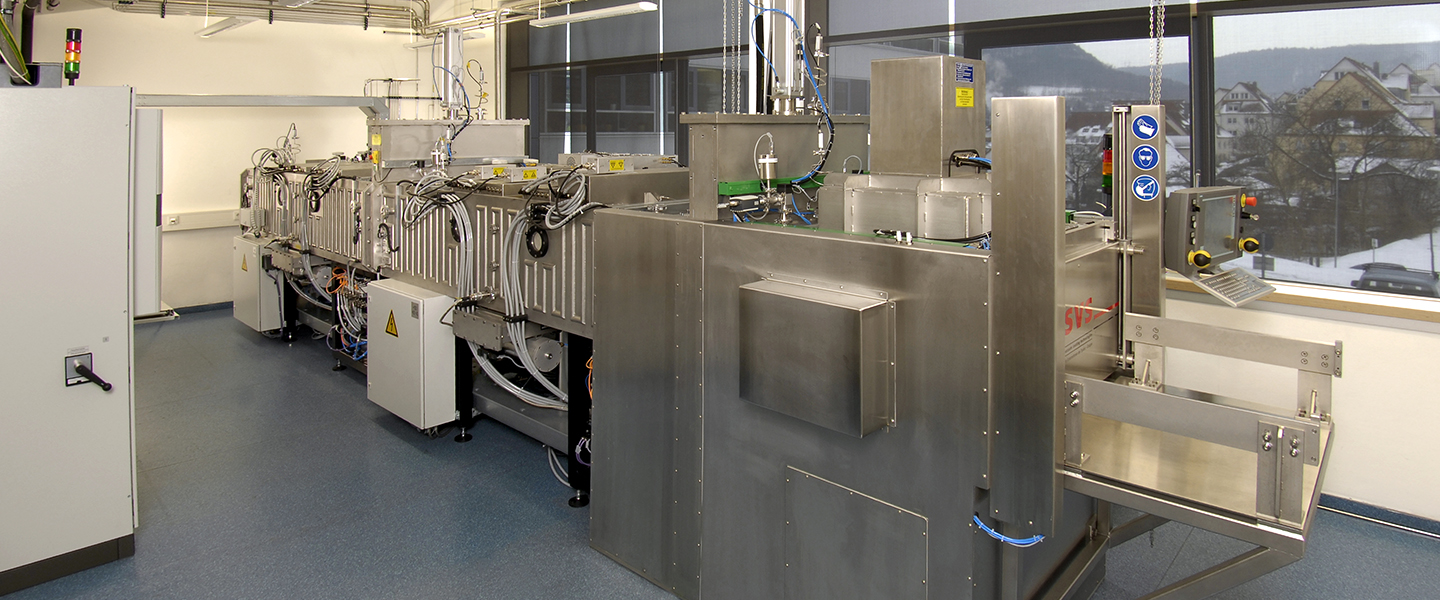
The group’s institutes have developed sputtering processes as one of its core technologies; these processes can be used to apply layers and multilayer systems onto large surfaces in a vacuum very efficiently. Sputtering processes are particularly suitable for the precise deposition of thin electrical and optical functional layers on an industrial scale. In this way, layer thickness accuracies, low roughness and good layer adhesion can be achieved.
Magnetron sputtering and the hollow cathode process are central technologies of the Fraunhofer IST for the production of various coatings. Magnetron sputtering is based on the principle of sputtering in low pressure glow discharges. In the cathode case, ions are thrown onto the cathode, so that in the cathode a collision cascade is excited, which leads to the triggering of target material. With the method of magnetic pressure increase, the working pressure of the sputtering process of about 5 Pa can be reduced without magnetic field to about 0.1 - 1 Pa. The hollow cathode glow discharge is a special form of low pressure glow discharge. It arises when the cathode takes the form of a hollow body and leads to significantly higher plasma densities.
Fraunhofer IOF uses magnetron sputtering on precision optics to meet the increasing demands on the quality and homogeneity of the coating on large optics. Classical sputtering systems are also used for the deposition of EUV/X-ray systems on substrate sizes up to ∅ 660 mm.
Fraunhofer FEP specializes in pulse magnetron sputtering (PMS) and regulating reactive sputtering processes. By using a pulse-shaped feed of the electrical energy during the magnetron gas discharge, the institute has been able to reduce disturbing arcing processes. Reactive process management can significantly expand the range of depositable materials: this way – in addition to metals – oxides, nitrides and oxynitrides can also be applied. Electrically highly insulating materials can also be deposited with the dual magnetron sputtering system (DMS), the bipolar technology version. Fraunhofer FEP focuses on developing the technology, adapting it to new applications and developing packages for complex integrated process technology and know-how.
209/5000For the deposition of nanometer enzel and multilayers for EUV and X-ray optics, the Fraunhofer IWS uses the methods of magnetron and ion beam sputter deposition as well as pulse laser deposition.

