- Functional layers and multi-material layer systems for sensors, electronics and optics
- Wear and corrosion protection layers for tools and components
- Tribological layers for highly stressed components
- Laser post-treatment of nano- and microparticulate layers
- Combination processes from wet-chemical coating processes (e.g. dip coating, rotary coating, inkjet, spraying, dispensing, screen printing, pad printing) and laser post-treatment
Thermoelectric Thin Layer Systems
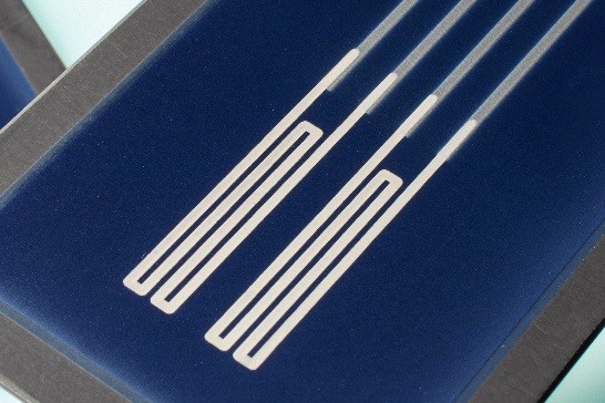
By using special technologies and process designs, the group’s institutes can produce functional components with thin layers. Thermoelectric (TE) components are traditionally made of solid materials. Fraunhofer IPM has developed the first wafer-based production process for thermoelectric converters with thin-film technology. Such converters are characterized by extremely high power densities and their improved dynamics enable precise, fast cooling.
Orangic-electric Thin Layer Systems
A far-reaching application of thin film processes, extending far beyond the use of classical coating technologies, is the production of organic semiconductor devices, as pursued at Fraunhofer FEP. Organic semi-finished materials enable the generation of large-area structural elements, for example organic light-emitting diodes (OLED) or organic solar cells on flexible carrier materials.
Modules on thin substrates, such as metal and polymer films or ultramodern flexible glass, can be used to create completely new lighting solutions (e.g. integrated into curved surfaces). The materials can be transparent, which is of particular importance to display industry and other consumer products). Applications are mainly found where design requirements are combined with efficiency and light weight, particularly in the automotive and aerospace industries, but this innovation can also be integrated into furniture, interior fittings and packaging.
Fraunhofer FEP has great competencies along the entire value-added chain for flexible OLED modules – from the bare substrate to integrated lights. The institute offers research and development services for all developments, including customer-specific layouts, at the prototype levels or in small series. The group has numerous processes and plants as well as several clean rooms at its disposal, enabling it to combine processes and conduct product development and innovation more effectively. In addition, it has various coating technologies, such as vacuum evaporation of organic and inorganic materials, atomic layer deposition (ALD), as well as printing and lamination processes and laser ablation. Many of these processes can be conducted and combined without a sudden loss of vacuum or under inert conditions.
These preparative technologies are supplemented by powerful measuring and characterization devices, which can be used to analyze OLED, solar cells and photodiodes electrically and optically.
Typical fields of application for organic semiconductor devices are as follows:
- OLEDs on flexible substrates (metal and polymer films, ultra-light flexible glass, ...)
- Flexible OLED lighting
- Organic photovoltaics (OPV)
- Organic photodiodes (OPD)
- Flexible solar modules
- Transparent solar cells
- OLED microdisplays
- OLED microstructures
- Color variable OLEDs

